Introduction
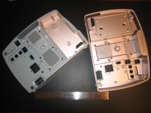
Medical devices are required to function flawlessly in noisy hospital environment or in wide range of home or doctor’s office settings. This issue is widely recognized as sizable concern by medical device manufacturers, its industry association and US federal government. Demand for smaller, more compact devices and lighter weight equipment drive medical device manufacturers to look increasingly at injection molded plastics to meet design requirements. Being non-conductive, plastic components do not shield electromagnetic interference (EMI) from being emitted from or penetrating an electronic device, and require shielding systems be incorporated to meet regulations and ensure reliable device performance. Conductive coatings essentially consume no volume inside an electronic device and if applied properly can assist the design engineer reliably meet cost budgets. Conductive coatings, first applied in electronic devices over 25 years ago, have demonstrated reliable and cost effective performance in laptop computers, cellular handsets, telecom switchgear, medical devices, military electronics, industrial equipment and a host of other electronic equipment that utilize injection molded plastic enclosures.
When designing products housed in injection molded plastic, a few key issues need to be comprehended when considering electromagnetic interference (EMI) shielding, including

- Selecting a resin that is compatible with the processes used to coat the plastic parts with metal,
- Determining what frequency range needs to be shielded,
- The relative amount of shielding required to meet emission limits set by the FCC and/or to protect the device from incoming interference in the field,
- Mechanical design of component that requires the shielding, and
- The operating environment that the coating will see in use (exposure to high temperatures, strong chemicals, fumes or gases and/or salt fog?)
This article will address the key design issues facing medical device engineers considering plastic with conductive coating to address EMI shielding requirements.
EMI Shielding Processes
All-Over Electroless and Electrolytic Plating
The starting point for plating on plastic is electroless plating where an initial layer of copper or nickel is deposited directly onto the plastic part. Electroless plating is an autocatalytic, chemical plating process which deposits a pure, continuous metal layer. The part is immersed into a series of plating tanks, including chemical etch to roughen the surface and activation to deposit a catalyst onto the part prior to deposition of copper. The etching and activation steps impact only the outer skin of the plastic. The bulk material properties of the plastic part are not affected. Electroless plating produces uniform thickness on all surfaces of plastic part, even in recesses and holes.
Once the electroless copper layer is deposited onto the plastic part, additional copper thickness can be deposited as required for EMI shielding performance and/or can be finished with nickel, tin or gold to provide the functional metal coating to meet the full range of mechanical, electrical, environmental and appearance requirements. Typically, electroless plating is used to deposit thin metal coatings, from 0.00004” (1.0 µm) to 0.0005” (12.5 µm). If thicker coatings are required, electrolytic plating (also called electroplating) can be used to deposit thicker coatings of copper, nickel, tin, chrome, silver, and gold over the electroless copper plated part. Electroplating deposits at faster rates and lower costs compared to the same thickness of electroless plating; however, electroplating is a line-of-sight process that will yield wider thickness variation over a part than would electroless plating. Electroplating process can be used to deposit from 0.0002” (5.0 µm) to 0.002” (50 µm) or more metal thickness. Also, electroplating is used to produce decoratively plated plastic parts with available finishes including nickel, bright chrome, and copper.
Selecting a plateable resin is among the most critical factors for a successful EMI shielding application. Table below lists common injection molded thermoplastic resins. It includes plateable as well as non-plateable resins, and some resin families that include both plateable and non-plateable grades. Some (but not all) non-plateable resins can be made plateable by custom blending a plating additive into the base resin. Examples of custom blending to produce plateable resins include polypropylene and polyphthalamide. Both resins are typically not plateable, but when custom blended with the plating additive, become plateable.
| Resin | All-Over Plating | Selective Plating |
|---|---|---|
| ABS | Yes | Yes |
| PC/ABS | Yes | Yes |
| PC | Yes | Yes |
| PEI/Ultem | Yes* | Yes |
| PEEK | Yes* | Yes |
| Polystyrene | Yes | Yes |
| Urethane | Yes | Yes |
| PPS | Limited | No |
| PPA | Custom Resins | Custom Resins |
| LCP | Yes* | No |
| * requires minimum 20-30% glass fill or media blasting prior to plating | ||
SLA’s and 3D printed parts can present challenges for plating due to low operating temperature and compatibly with plating process. Plastic resins require heat deflection temperature of at least 170F (76C). To date only a few 3D printed grades are viewed as routinely plateable, ABS, ABSplus and Visijet M3X.
Plating can be applied over the entire part as described above, or selectively, onto specified areas.
Selective Autocatalytic Plating Catalyst
 Spray plating catalyst onto the areas of the plastic part using custom built paint masks to control the location of the catalyst. When the catalyzed parts are immersed into electroless copper tank, the chemical make-up of the catalyst draws copper metal out of the plating solution and deposit copper uniformly onto the catalyzed area. Following electroless copper plating, electroless nickel plating can be applied to protect the copper from corrosion and abrasion. The plating catalyst thickness is approximately 0.001” (0.025 mm), and the electroless plating thickness is limited to 0.0001” (2.5 µm) to 0.00025” (6.25 µm). The plastic parts are never exposed to aggressive chemistries; therefore, the molded-in-color and texture of the plastic part are maintained through the process.
Conductive Paint
 Conductive paints are comprised of micron sized metal particles of nickel, copper, silver plated copper or silver blended into water or solvent based paint system. Similar to selective plating process, a masking fixture is used to control the location of the conductive paint that is sprayed onto the required areas of the part. The fully cured conductive paint thickness ranges from 0.0005” (0.0125 mm) to 0.002” (0.05 mm) depending on the paint type and EMI shielding requirement. The paint can be applied in a manual paint booth where an operator applies the paint with a paint gun or with a paint robot. The paint robot offers advantages over manual spray methods, especially in higher volume applications where cost is critical. In the robot, the spray pattern can be programmed and frozen to apply the optimal amount of conductive paint across the entire shielded surface. Manual paint application typically has lower set-up cost than robotic painting and is a good match with lower volume applications.
Paintable Plastic Resins |
||
|---|---|---|
| ABS | Polycarbonate (PC) | Polybutylene Terephthalate (PBT) |
| PC/ABS | Poly Aryl Amide | Noryl Polyphenylene Oxide (PPO) |
| ASA | Polyphthalamide (PPA) | Ultem - Polyetherimide (PEI) |
| Nylon | Polystyrene (PS) | Xenoy (PC/PBT) |
Difficult to Paint Resins (May Require Prime or not Paintable) |
||
| PVC | Polyethylene | Liquid Crystal Polymer (LCP) |
| PEEK | Polyimide | Polypropylene (PP) |
| PPS | PES | Polyester |
Shielding Requirements and Shielding Effectiveness
Designing for EMI shielding is best done up front, early in the product design cycle. Designing the electronics, the plastic enclosure and EMI shielding system simultaneously as opposed to sequentially can reduce the time-to-market as well as production cost.
The basic EMI shielding principal, also known as the Faraday Cage Principal, is well understood; however, applying the principal to electronic equipment design can present challenges to engineers. Ultimately, compliance to regulations as well as performance in the end use environment needs to be confirmed with fully assembled systems being subjected to EMI testing in a lab. A few guidelines for EMI shielding coatings can assist the engineer in specifying a coating that will meet the requirements. EMI can be divided into 2 broad categories, magnetic and electric. Magnetic interference is generally viewed as less than 30 MHz frequency where electric interference is 30 MHz and above. To shield longer wavelength magnetic interference, thicker coatings that include magnetic materials such as nickel are preferred. For electric interference, thin conductive coatings comprised of copper or silver typically perform best. In many cases, the conductive metal thickness can be as thin as 1 micron for applications with frequency >30 MHz.
| Attenuation (dB) | ||||||||
|---|---|---|---|---|---|---|---|---|
| Coating System | Thickness | (m-ohms/square) Resistivity | 30 MHz | 100 MHz | 300 MHz | 1 GHz | 5 GHz | 10 GHz |
| All-Over Copper/Nickel Plating | 40-100 µ” (1.0-2.5 µm) | 5-50 | 90 | 108 | 104 | 120 | 113 | 87 |
| Selective Copper/Nickel Plating | 80-100 µ” (2.0-2.5 µm) | 25-100 | 77 | 73 | 71 | 71 | 60 | 63 |
| Silver Plated Copper Paint | 0.001-.0015” (0.025-.375 mm) | 25-100 | 65 | 63 | 59 | 70 | 81 | 63 |
| Silver Plated Copper-Silver Paint | 0.0008-.001” (0.020-.25 mm) | 15-50 | 78 | 73 | 72 | 69 | 85 | 82 |
| Silver Paint | 0.0005-.001” (0.0125-.025 mm) | 15-50 | 70 | 71 | 70 | 62 | 70 | 70 |
Part Design Considerations
As with resin selection, plastic part design is critical to successful application. There are design approaches that should be avoided if possible.
| Design Don't | Design Alternative |
|---|---|
| 5-sided box or cup design that can trap air and/or drag out plating chemicals, impacting plating quality and cost | Include drain holes or design part to prevent entrapment of air or plating solution. |
| Tight crevices that can trap plating solution | Eliminate crevices in the design or include drain hole. |
| Small blind holes can trap plating solution that can later weep out and damage the plating. | Utilize through-holes if possible. If blind holes are required, they can be plugged to prevent plating solution entrapment. |
| Design Don't | Design Alternative |
|---|---|
| Difficult to paint tight bosses, crevices and holes due to line-of-sight process to apply paint | Eliminate crevices and small holes that require coating |
Environmental Factors for EMI Shielding Coating
The operating environment is also a critical factor to be comprehended in the design of the part and the EMI shielding coating. The selection of the EMI coating system will be a function of the EMI shielding requirement (frequency range and required attenuation). Another factor that must be considered is the environment that the EMI shielding will see. If the shielding will need to operate with exposure to strong chemicals used in the operation or cleaning of the device, is exposed to gases or fumes in use, and/or is used in outdoor setting where salt fog could penetrate the device, the potential corrosion of the EMI shielding needs to be considered. For harsh operating environments, it is recommended to consider plating as leading option and to increase nickel plating thickness so that the underlying copper plating is protected. If conductive paint is the preferred route, nickel paint may be an option compared to copper paint. Silver plated copper paint will offer improved corrosion resistance compared to copper paint although still not equivalent to nickel paint in many harsh operating conditions. Silver paint is a further improvement over silver plated copper paint but is very costly due to the filler being pure silver.
Summary
Designing for EMI shielding is best accomplished early in the medical device design cycle before such key issues as plastic resin selection and final part design are finalized. Shielding systems can be tailored to be highly cost effective as well as to provide critical EMI shielding performance in medical devices and military electronics.

